
Xilinx design flow and project setup
Getting the IDE and license:Used tool: ISE Design Suite V14.7
This tool-set can be downloaded from the Xilinx website: Link Select tab "ISE design tools"
It is possible to get a free permanent "Webpack" license from Xilinx, create an account on the Xilinx website and by mail you get the free Webpack license file.
Start the ISE Design suite.
On the toolbar, select Help->Manage license
Specify the location of the .lic file in the field 'LM_LICENSE_FILE' and click 'Set'
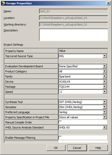
| Project setup: On the toolbar, select File->New project Specify a project name and a location on your disk, click Next and specify the settigns as shown in the screenshot for: - Family - Device - Package - Speed Create a toplevel Module: Use the context menu and select "Create new source" 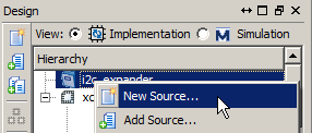 Select the source type and file name: This depends on your preference: I've used: - Verilog Module Note: make sure the box "Add to project" is checked. |
 |
To test if the tool chain is functional we just recreate the blinking led application.
The toolchain contains these parts:
- Define a project (as described above)
- Input of the code
- Defining contstraints (basically pin mapping + clock definition)
- Synthesize + Mapping and Routing
- Generation of a bit file
- Transfer the bit file to the FPGA
Input of the code:
As a test this small file is used
`timescale 1ns / 1ps
//////////////////////////////////////////////////////////////////////////////////
// Company:
// Engineer:
//
// Create Date: 19:45:20 06/29/2014
// Design Name:
// Module Name: top
// Project Name:
// Target Devices:
// Tool versions:
// Description:
//
// Dependencies:
//
// Revision:
// Revision 0.01 - File Created
// Additional Comments:
//
//////////////////////////////////////////////////////////////////////////////////
module top(
input clk,
output [1:0] out,
input reset
);
// clk OSC_FPGA50MHzPin 85
// n.a. PB11: Button not pressed, 0: button pressed Pin 101
// reset PB01: Button not pressed, 0: button pressed Pin 102
// out[1] LED11: Led on, 0: Led off Pin 104
// out[0] LED01: Led on, 0: Led off Pin 105
reg [26:0] cnt_val;
always @(posedge clk)
begin: COUNTER
if (~reset) begin
cnt_val <= 26'b0;
end
else begin
cnt_val <= cnt_val+1;
end
end
assign out[0] = cnt_val[24];
assign out[1] = cnt_val[26];
endmodule
Defining the constraints:
Use the context menu in the hierarchy view: New source -> Implementation Constraint File
You may also chose to use the constaints editor (found in the Toolbar, under section 'Tools')
The result should be a .ucf fiel with this content:
TIMESPEC TS_clk = PERIOD "clk" 20 ns HIGH 50%;
NET "OUT<0>" LOC = "P105" |IOSTANDARD = LVTTL;
NET "OUT<1>" LOC = "P104" |IOSTANDARD = LVTTL;
NET "CLK" LOC = "P85" |IOSTANDARD = LVTTL;
NET "RESET" LOC = "P102" |IOSTANDARD = LVTTL;
NET "clk" TNM_NET = clk;
Synthesize, Mapping & Routing:
Press the green 'Play' button or use the Toolbar -> Process -> Run, Rerun or Rerun All
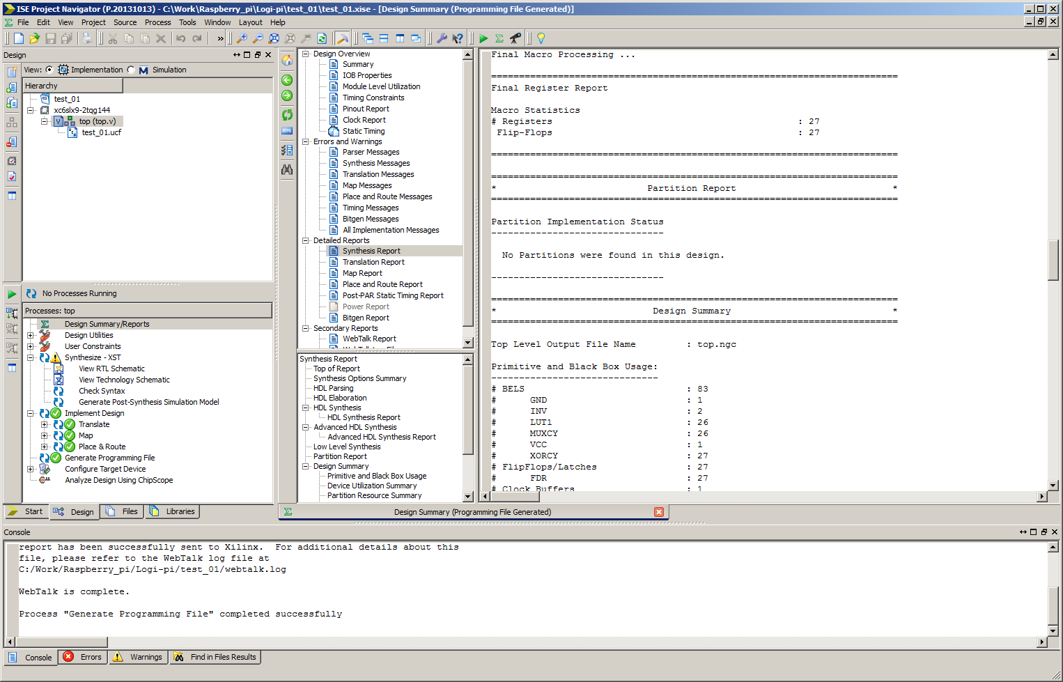
There are several items which you might check, see the Error and Warnings, the Console output and the different reports. For instance, select 'Design Summary/Report' in the 'Design' Tab of the 'Process' Pane.. Open the 'Synthesis Report': This report shows you how many FlipFlops and other resources are used. It is good to check that this design uses 27 FlipFlops, which you may expect given the reg[26:0] definition in the source code where also bit 26 is used. Unused bits would be optimized, meaning the systhesis tool throws them away. Further we did not accidentally create latches, which is good to check.
There is one warning: HDLCompiler: 413 = Result of 28 bit expression is truncated to fit in 27 bit target.
This is correct: The increment of the counter value is an adder. Adding an n bit value results in and n+1 bit result, but we store the value in the same counter register, thus theoretically we throw away information, which is the roll-over of the counter. If we would have meant an adder, then this warning is a serious item to check.
Generation of a bit file:
Double click the 'Generate Programming file' in the 'Process' Pane. The result is the .bit file.
Transfer the bit file to the FPGA:
A convenient way is to use an SCP client, such as WinSCP.exe.
Final step is to transfer the file to the FPGA:
>sudo logi_loader <bitfilename>.bit